- 您现在的位置:买卖IC网 > Sheet目录330 > IDT71V256SA20PZG (IDT, Integrated Device Technology Inc)IC SRAM 256KBIT 20NS 28TSOP
IDT71V256SA
3.3V CMOS Static RAM 256K (32K x 8-Bit)
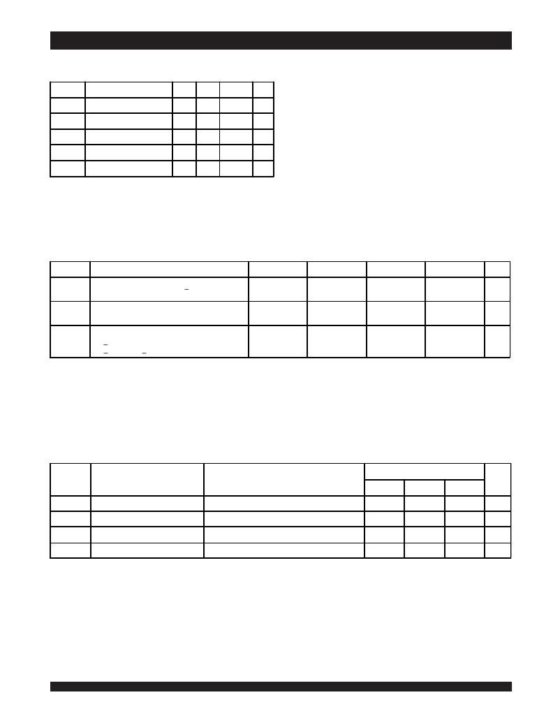
Recommended DC Operating
Conditions
Commercial and Industrial Temperature Ranges
-0.3
Symbol
V CC
GND
V IH
V IH
V IL
Parameter
Supply Voltage
Ground
Input High Voltage - Inputs
Input High Voltage - I/O
Input Low Voltage
Min.
3.0
0
2.0
2.0
(1)
Typ.
3.3
0
____
____
____
Max.
3.6
0
V CC +0.3
V CC +0.3
0.8
Unit
V
V
V
V
V
NOTE:
1. V IL (min.) = –2.0V for pulse width less than 5ns, once per cycle.
3101 tbl 06
DC Electrical Characteristics (1)
(V CC = 3.3V ± 0.3V, V LC = 0.2V, V HC = V CC - 0.2V, Commercial and Industrial Temperature
Ranges)
Symbol Parameter 71V256SA10 71V256SA12 71V256SA15 71V256SA20
Unit
I CC
I SB
I SB1
Dynamic Operating Current CS < V IL , Outputs
Open, V CC = Max., f = f MAX (2)
Standby Power Supply Current (TTL Level)
CS = V IH , V CC = Max., Outputs Open, f = f MAX (2)
Full Standby Power Supply Current (CMOS Level)
CS > V HC , V CC = Max., Outputs Open, f = 0 (2) ,
V IN < V LC or V IN > V HC
100
20
2
90
20
2
85
20
2
85
20
2
mA
mA
mA
NOTES:
1. All values are maximum guaranteed values.
2. f MAX = 1/t RC , only address inputs cycling at f MAX ; f = 0 means that no inputs are cycling.
DC Electrical Characteristics
(V CC = 3.3V± 0.3V)
IDT71V256SA
3101 tbl 07
Symbol
|I LI |
|I LO |
V OL
V OH
Parameter
Input Leakage Current
Output Leakage Current
Output Low Voltage
Output High Voltage
Test Conditions
V CC = Max., V IN = GND to V CC
V CC = Max., CS = V IH , V OUT = GND to V CC
I OL = 8mA, V CC = Min.
I OH = -4mA, V CC = Min.
Min.
___
___
___
2.4
Typ.
___
___
___
___
Max.
2
2
0.4
___
Unit
μA
μA
V
V
3101 tbl 08
3
6.42
发布紧急采购,3分钟左右您将得到回复。
相关PDF资料
IDT71V25761S200PFGI
IC SRAM 4MBIT 200MHZ 100TQFP
IDT71V30L35TFI
IC SRAM 8KBIT 35NS 64STQFP
IDT71V321L25TFI
IC SRAM 16KBIT 25NS 64STQFP
IDT71V3556SA166BGGI
IC SRAM 4MBIT 166MHZ 119BGA
IDT71V3559S85BQI
IC SRAM 4MBIT 85NS 165FBGA
IDT71V35761YSA200BGI
IC SRAM 4MBIT 200MHZ 119BGA
IDT71V3577S75BQG
IC SRAM 4MBIT 75NS 165FBGA
IDT71V3578S150PFGI
IC SRAM 4MBIT 150MHZ 100TQFP
相关代理商/技术参数
IDT71V256SA20PZG8
功能描述:IC SRAM 256KBIT 20NS 28TSOP RoHS:是 类别:集成电路 (IC) >> 存储器 系列:- 标准包装:72 系列:- 格式 - 存储器:RAM 存储器类型:SRAM - 同步 存储容量:4.5M(256K x 18) 速度:133MHz 接口:并联 电源电压:3.135 V ~ 3.465 V 工作温度:0°C ~ 70°C 封装/外壳:100-LQFP 供应商设备封装:100-TQFP(14x20) 包装:托盘
IDT71V256SA20PZGI
功能描述:IC SRAM 256KBIT 20NS 28TSOP RoHS:是 类别:集成电路 (IC) >> 存储器 系列:- 标准包装:72 系列:- 格式 - 存储器:RAM 存储器类型:SRAM - 同步 存储容量:4.5M(256K x 18) 速度:133MHz 接口:并联 电源电压:3.135 V ~ 3.465 V 工作温度:0°C ~ 70°C 封装/外壳:100-LQFP 供应商设备封装:100-TQFP(14x20) 包装:托盘
IDT71V256SA20PZGI8
功能描述:IC SRAM 256KBIT 20NS 28TSOP RoHS:是 类别:集成电路 (IC) >> 存储器 系列:- 标准包装:72 系列:- 格式 - 存储器:RAM 存储器类型:SRAM - 同步 存储容量:4.5M(256K x 18) 速度:133MHz 接口:并联 电源电压:3.135 V ~ 3.465 V 工作温度:0°C ~ 70°C 封装/外壳:100-LQFP 供应商设备封装:100-TQFP(14x20) 包装:托盘
IDT71V256SA20PZI
功能描述:IC SRAM 256KBIT 20NS 28TSOP RoHS:否 类别:集成电路 (IC) >> 存储器 系列:- 产品变化通告:Product Discontinuation 05/Nov/2008 标准包装:84 系列:- 格式 - 存储器:RAM 存储器类型:SRAM - 同步 ZBT 存储容量:4.5M(128K x 36) 速度:75ns 接口:并联 电源电压:3.135 V ~ 3.465 V 工作温度:-40°C ~ 85°C 封装/外壳:119-BGA 供应商设备封装:119-PBGA(14x22) 包装:托盘 其它名称:71V3557SA75BGI
IDT71V256SA20PZI8
功能描述:IC SRAM 256KBIT 20NS 28TSOP RoHS:否 类别:集成电路 (IC) >> 存储器 系列:- 产品变化通告:Product Discontinuation 05/Nov/2008 标准包装:84 系列:- 格式 - 存储器:RAM 存储器类型:SRAM - 同步 ZBT 存储容量:4.5M(128K x 36) 速度:75ns 接口:并联 电源电压:3.135 V ~ 3.465 V 工作温度:-40°C ~ 85°C 封装/外壳:119-BGA 供应商设备封装:119-PBGA(14x22) 包装:托盘 其它名称:71V3557SA75BGI
IDT71V256SA20Y
功能描述:IC SRAM 256KBIT 20NS 28SOJ RoHS:否 类别:集成电路 (IC) >> 存储器 系列:- 产品变化通告:Product Discontinuation 05/Nov/2008 标准包装:84 系列:- 格式 - 存储器:RAM 存储器类型:SRAM - 同步 ZBT 存储容量:4.5M(128K x 36) 速度:75ns 接口:并联 电源电压:3.135 V ~ 3.465 V 工作温度:-40°C ~ 85°C 封装/外壳:119-BGA 供应商设备封装:119-PBGA(14x22) 包装:托盘 其它名称:71V3557SA75BGI
IDT71V256SA20Y8
功能描述:IC SRAM 256KBIT 20NS 28SOJ RoHS:否 类别:集成电路 (IC) >> 存储器 系列:- 产品变化通告:Product Discontinuation 05/Nov/2008 标准包装:84 系列:- 格式 - 存储器:RAM 存储器类型:SRAM - 同步 ZBT 存储容量:4.5M(128K x 36) 速度:75ns 接口:并联 电源电压:3.135 V ~ 3.465 V 工作温度:-40°C ~ 85°C 封装/外壳:119-BGA 供应商设备封装:119-PBGA(14x22) 包装:托盘 其它名称:71V3557SA75BGI
IDT71V256SA20YG
功能描述:IC SRAM 256KBIT 20NS 28SOJ RoHS:是 类别:集成电路 (IC) >> 存储器 系列:- 产品变化通告:Product Discontinuation 05/Nov/2008 标准包装:84 系列:- 格式 - 存储器:RAM 存储器类型:SRAM - 同步 ZBT 存储容量:4.5M(128K x 36) 速度:75ns 接口:并联 电源电压:3.135 V ~ 3.465 V 工作温度:-40°C ~ 85°C 封装/外壳:119-BGA 供应商设备封装:119-PBGA(14x22) 包装:托盘 其它名称:71V3557SA75BGI
